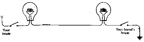
It's possible to reduce to just one the number of wires in a bidirectional telegraph, but the reduction comes at a cost:
The downside of this circuit is that you and your friend can’t send messages to each other simultaneously. To receive a message from your friend, the switch on your end must be depressed. Your friend’s switch then turns both lights on and off. Similarly, when you want to send a message, your friend’s switch must be depressed. If either switch is open, the light bulbs can’t be lit. Because both light bulbs are always lit at the same time, twice as many batteries are needed; otherwise the bulbs would be a little dim. Because this configuration is more difficult to use than the two-wire version, it’s probably not preferable even if it does save on wire.
There's actually a cheaper way to make a AND gate out of relays, requiring only one relay rather than two:
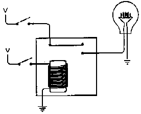
However, it's best if the output of relays is a full V. In this alternate configuration, if the top input is not a switch connected to V, the output may be less than V.
| A input: | 0 | 0 | 1 | 1 | Output Description |
|---|---|---|---|---|---|
| B input: | 0 | 1 | 0 | 1 | |
| Output Bits | |||||
| Gate 0: | 0 | 0 | 0 | 0 | Ground |
| Gate 1: | 0 | 0 | 0 | 1 | A AND B |
| Gate 2: | 0 | 0 | 1 | 0 | A AND NOT B |
| Gate 3: | 0 | 0 | 1 | 1 | A |
| Gate 4: | 0 | 1 | 0 | 0 | NOT A AND B |
| Gate 5: | 0 | 1 | 0 | 1 | B |
| Gate 6: | 0 | 1 | 1 | 0 | A XOR B |
| Gate 7: | 0 | 1 | 1 | 1 | A OR B |
| Gate 8: | 1 | 0 | 0 | 0 | A NOR B |
| Gate 9: | 1 | 0 | 0 | 1 | A EQU B |
| Gate 10: | 1 | 0 | 1 | 0 | NOT B |
| Gate 11: | 1 | 0 | 1 | 1 | A OR NOT B |
| Gate 12: | 1 | 1 | 0 | 0 | NOT A |
| Gate 13: | 1 | 1 | 0 | 1 | NOT A OR B |
| Gate 14: | 1 | 1 | 1 | 0 | A NAND B |
| Gate 15: | 1 | 1 | 1 | 1 | Voltage |
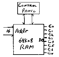
The eight bits of the output of the Code RAM array can be referred to as C0 (the least significant bit of the code), C1, C2, C3, C4, C5, C6, and C7 (the most significant bit):
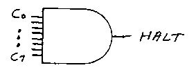
Our job will be a little easier if we decode these signals for the operations they represent. For example, the output of this 8-input AND gate will be 1 if the operation code is a Halt:
Similarly, this 8-input NOR gates can provide a signal called LOAD:
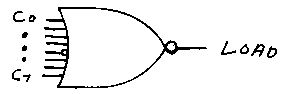
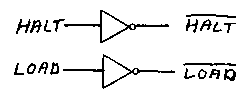
Note the little circle on the C4 input that indicates that the signal is being inverted. Similar configurations can provide signals called STORE and ADD. And signals can be inverted like so:
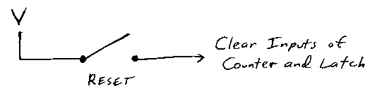
As in the earlier circuit, a switch is attached to the clear inputs of the 16-bit counter and the 8-bit latch. But now I’m going to call this switch the Reset switch:
An oscillator provides a Clock signal for the 16-bit counter and the latch, but now that Clock signal is 0 if the output of the Code RAM array is the Halt code:
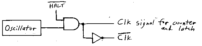
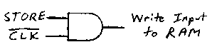
The inverse of the Clock signal is the Write input to the Data RAM array, but only if the operation is a Store:
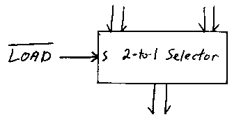
Finally, the Select input to the 2-Line-To-1-Line Data Selector should be 0 if the operation is Load and 1 otherwise:
And that’s it.
You begin using this automated adder by entering all the numbers and operations codes into the two RAM arrays. Let’s assume you entered the values shown earlier. At the outset, the Reset switch is closed so the Reset signal in the timing diagram is 1. The counter output is 0000h, so the output of the Code RAM array is the value at the 0000h address, which is 10h. The output of the Data RAM array is the value 27h. The 10h output from the Code RAM array causes the select input to the 2-Line-To-1-Line Data Selector to be 0. The latch input is thus the output of the Data RAM array, which is 27h. The latch output is 00h because the clear signal (which is the Reset switch) is 1.
A timing diagram of some of this circuit might clarify how it works. When you open the Reset switch, things start moving:
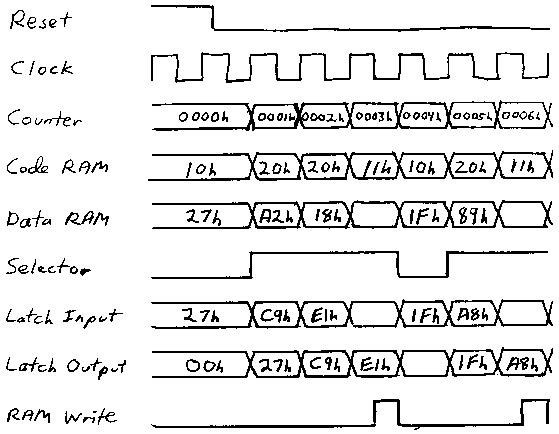
At the next positive transition of the Clock signal after the Reset signal becomes 0, the latch output becomes 27h. The counter increments to 0001h. The output of the Code RAM array is 20h (the Add operation) and the output of the Data RAM array is A2h. The select input to the 2-Line-To-1-Line Data Selector is 1, which means that the input to the latch is the sum of the output of the Data RAM array (A2h) and the latch output (27h), or C9h.
At the next positive transition of the Clock signal, the counter increments to 0002h, and the latch output becomes C9h. The output of the Code RAM array is again 20h, and the output of the Data RAM array is the third number, 18h. The input to the latch is the sum of that value and the latch output, which is now C9h. That sum is E1h.
At the next positive transition of the clock signal, the counter increments to 0003h, and the latch output becomes E1h. The output of the Code RAM array is 11h, which is the code for the Store operation. The output of the Data RAM array is not important, which is why it’s shown in the timing diagram as a blank. Nor is the input to the latch important. What’s important is the output of the latch, which is connected to the data inputs of the Data RAM array. The RAM write signal writes that value into memory.
Similarly, the timing diagram also shows the second addition.
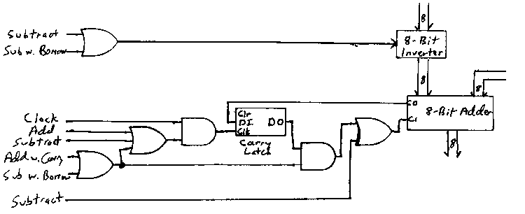
The following can be inserted following the table of operation codes:
I demonstrated earlier how 8-input AND gates or NOR gates can be wired up to produce signals that correspond to each opcode. For example:
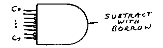
Notice that C2, C3, C4, C6, and C7 are inverted before being inputs to the AND gate. The output of the 8-input AND gate will be 1 only if the operation code is 23h (Subtract with Borrow). Similarly, signals corresponding to the other operation codes can be generated. Adding the carry latch to implement these two new operation codes is a little messy but doesn’t involve an inordinate amount of new components:
The following can be inserted following the illustration:
As usual, the hard part is the little stuff--all those clocking signals and whatnot known collectively as the control signals. I won’t show the detailed control signals fpr this and future configurations. (Nor will I be sadistic enough to categorize this an “exercise for the reader”!) But I will show you a very handy tool for generating complex control signals. This is known as a ring counter.
You may recall the edge-triggered D-type flip-flop with preset and clear that we encountered at the end of Chapter 14:
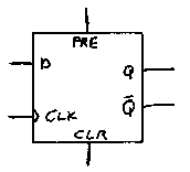
Normally, the Preset and Clear inputs are set to 0. Then, whenever the Clock input goes from 0 to 1, the Q output becomes the same as the Data input. When the Clear input is 1, then the Q output is 0, and when the Preset input is 1, then the Q output is 1:
| Inputs | Outputs | ||||
|---|---|---|---|---|---|
| Preset | Clear | D | Clk | Q | Q-bar |
| 1 | 0 | X | X | 1 | 0 |
| 0 | 1 | X | X | 0 | 1 |
| 0 | 0 | 0 | up-arrow | 0 | 1 |
| 0 | 0 | 1 | up-arrow | 1 | 0 |
| 0 | 0 | X | 0 | Q | Q-bar |
You can make a 4-bit ring counter by connecting four of these flip-flops like so:
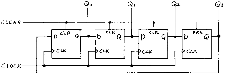
Notice that a single Clock signal serves to clock all four flip-flops. Also notice that the Q output of each flip-flop is the D input of the next flip-flip. In fact, the Q output of the fourth flip-flip at the right is the D input of the first flip-flop at the right. A single Clear signal is connected to the Clear inputs of the first three flip-flops, and the Preset input of the fourth. Therefore, when the Clear signal is 1, then Q0, Q1, and Q2 are all 0 and Q3 is 1. When Clear goes to 0, then the Clock causes the outputs of the flip-flips to change as shown in the following timing diagram:
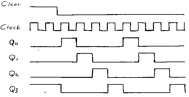
First Q0 is 1, then Q1 is 1, then Q2, then Q3, and back again to Q0.
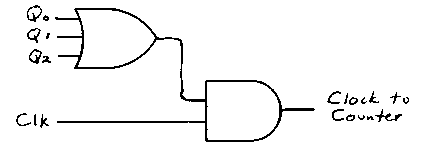
Q0 can be used as the clock input of the top 8-bit latch--the one that holds the instruction code from the Code RAM. Q1 is the clock input of the middle 8-bit latch, which holds the high-order byte of the 16-bit address, and Q2 is the clock input of the bottom 8-bit latch, which holds the low-order byte of the 16-bit address. Q3 can be the clock input to the accumulator latch. During this time, the 16-bit counter needs to advance three times because each instruction is three bytes in length. The clock to the 16-bit counter can be:
© Charles Petzold, 2000
code@charlespetzold.com
This page last updated January, 2000.